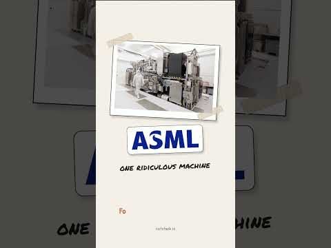
ASML has convinced TSMC, Samsung and Intel Foundry to jointly make the switch from six-inch to twelve-inch photomasks. The larger masks are expected to increase the throughput of ASML's High-NA EUV machines by 40 percent, according to ASML chief technology officer Marco Pieters. Production use of those twelve-inch masks is planned for 2033, with a joint test line that ASML and TSMC aim to build by 2031.
Meanwhile, Huawei is developing a Chinese counter-strategy. The technology giant is acting as an informal project manager within the Chinese DUV industry, providing financial backing to local equipment makers and helping them secure contracts with major chip manufacturers. The gap with ASML remains substantial for now, but the efforts signal how seriously China is pursuing the development of its own semiconductor supply chain.
Larger masks set to resolve bottleneck in High-NA EUV
ASML's High-NA EUV machines cost up to $400 million each and are considered the most advanced lithography systems in the world. The current six-inch photomasks represent a practical bottleneck for the production capacity of these machines. By switching to twelve-inch masks, chipmakers can expose more patterns per unit of time, significantly increasing machine efficiency.
Marco Pieters described the transition as a "tremendous opportunity." The willingness of TSMC, Samsung and Intel to co-invest in the development of an entirely new mask format is notable: such a transition requires adjustments throughout the entire production chain, from mask makers to the machines themselves.
The three chipmakers are at different stages in their adoption of High-NA EUV. Intel is already deploying the technology for selected layers of its 18A-based processors and has processed more than one million wafers using High-NA EUV. Samsung plans to use the machines for large-scale DRAM production from 2028. TSMC is targeting implementation in advanced nodes from 2030. SK Hynix is still evaluating whether to join the consortium. TSMC accounts for approximately 16 percent of ASML's total revenue.
Huawei as the pivot of China's DUV industry
While ASML strengthens its position with the largest chipmakers, Huawei is building an alternative for the Chinese market. The company is focusing on Deep Ultraviolet lithography, the generation of machines ASML has been producing for decades and on which export restrictions are also being steadily tightened.
Shanghai-based Yuliangsheng, founded in 2022 in the Pudong New Area, was a key contributor to the development of the first Chinese advanced DUV system. That system is currently being tested at chipmaker SMIC and on Huawei's own production lines. Yuliangsheng aims to produce twelve of these machines by the end of 2026.
In terms of capability, the machines are comparable to ASML's NXT:1980Di, a tool for 28-nanometer processes that can reach 7 nanometers with multi-patterning. That is, depending on the metric used, ten to fifteen years behind the international frontier. SMIC is evaluating the tool and is using multi-patterning to achieve 7nm-class production.
Huawei's investment arm Hubble has backed more than sixty Chinese semiconductor companies since 2019. In 2023, Hubble and a second Huawei-backed fund invested approximately 100 million renminbi (roughly $15 million) in Fujian Zhiqi Photonics, a manufacturer of ultra-precise optics, for a 37 percent stake. RSLaser, which develops light sources for older SMEE DUV tools, also receives support. He Tingbo, head of Huawei's chip division, oversees this network.
Technical dependencies remain a bottleneck
China's DUV development faces persistent technical obstacles. The projection lenses in Yuliangsheng's machines rely on glass from Germany's Zeiss, which supplies its optics exclusively to ASML. Analysts say lenses are being sourced on the secondary market, but this is not a structurally sustainable solution for large-scale production. The light source market is dominated by US-based Cymer and Japan's Gigaphoton, both beyond the reach of Chinese alternatives.
Meanwhile, existing production facilities in China, including those of Huawei itself, remain heavily dependent on ASML equipment. Huawei claims to have designed and produced 381 chips over the past six years, and is targeting production of 1.4-nanometer chips by 2031. Whether that is achievable without access to advanced Western lithography machines remains an open question.
Semiconductor analyst Lin Qingyuan of Bernstein is closely monitoring the Chinese efforts. China's share of ASML's net system sales fell from 19 percent in the first quarter of 2026 to 14 percent in the second quarter, partly as a result of tightened export controls.
What this means for the European semiconductor industry
ASML's ability to commit the three largest chipmakers to a shared mask standard illustrates how central the Veldhoven-based company is to the global chip production chain. Such a transition not only deepens relationships with existing customers but also raises the barrier for any potential future competitors.
For European policymakers and investors, the two developments together illustrate a structural tension that will not disappear in the years ahead. Export controls on advanced lithography machines are accelerating Chinese investment in local alternatives, while ASML continues to strengthen its position with the frontrunners of the chip industry. The question for the European ecosystem is how quickly Chinese DUV capacity will mature and what consequences that will have for the supply chains of companies such as ASML, Zeiss and the dozens of European suppliers that depend on that chain.