ASML and TNO are jointly building a pilot line for the mass production of photonic chips in Eindhoven. ASML will supply DUV and I-line lithography machines and provide process support. The facility will be constructed directly behind the existing SMART Photonics building on High Tech Campus Eindhoven and is set to be operational in 2027. The first chips are expected in 2028.
The partnership was announced on 24 June 2026. Financial details of the deal between ASML and TNO have not been disclosed. The broader pilot line represents an investment of over 153 million euros, funded by the European Union, the Dutch Ministries of Economic Affairs and Defence, TNO itself, and PhotonDelta, which is contributing 53 million euros from the National Growth Fund.
The collaboration is a public-private arrangement also involving Eindhoven University of Technology, the University of Twente, SMART Photonics and High Tech Campus Eindhoven. Within this framework, TNO, TU/e and the University of Twente are working together through the jointly established Photonic Integration Technology Centre (PITC). The project falls under the European PIXEurope programme.
From 4-inch to 6-inch wafers
The pilot line focuses on indium phosphide (InP) photonic chips on 6-inch wafers, a step forward compared with the current 4-inch wafer standard in this segment. The intended capacity will ultimately scale up to around 10,000 wafers per year.
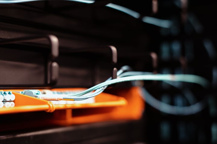
Photonic chips process data signals using light rather than electric current. They are used in data centres, medical equipment, sensors and telecoms infrastructure. The move to larger wafers lowers the production cost per chip and makes scaling up commercially more viable.
Access for companies, researchers and start-ups
TNO will operate the facility itself for the first five years, after which a potential transfer to industry is envisaged. Companies, researchers and start-ups will have access to the line, giving the factory an open-access character for parties that cannot build their own production facility.
Arnaud de Jong, Managing Director TNO High Tech Industry, emphasises that the collaboration with ASML is aimed at refining manufacturing processes in addition to the supply of machines. Stanislas Baron, Senior Vice President at ASML, points to the importance of European photonics infrastructure for the broader semiconductor industry.
Growing market for photonics
The global silicon photonics market is currently estimated at 278 million dollars and, according to market forecasts, could grow to 2.7 billion dollars by 2030, a compound annual growth rate of 46 per cent. Indium phosphide, on which the Eindhoven line is focused, has different properties from silicon photonics and is particularly suited to applications requiring light generation, such as lasers and optical amplifiers.
PhotonDelta, the consortium that organises the Dutch photonics ecosystem, is contributing financially and is involved as a partner. CEO Eelko Brinkhoff sees the pilot line as a link between fundamental research and industrial production. TNO CEO Tjark Tjin-A-Tsoi and Gerwin Gelinck, honorary professor of Integrated Photonics at the University of Twente, are also connected to the project.
European context and significance for the ecosystem
The collaboration fits within a broader European strategy to make critical technologies, including advanced semiconductors and photonics, less dependent on production outside Europe. For the Dutch ecosystem centred on Eindhoven, where ASML, SMART Photonics and PhotonDelta are already based, the pilot line adds a manufacturing link that was previously missing. This makes the region more attractive to photonics start-ups that currently depend on facilities elsewhere in the world for fabrication. For investors in the European photonics segment, an accessible, local pilot line provides greater opportunities to guide portfolio companies through the phase between prototype and series production.