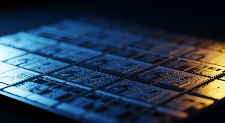
Intel has taken a new step in its chip manufacturing strategy. The company announced that 18A-P, a refined version of the 18A manufacturing process, has reached the risk production phase. In the semiconductor industry, this phase represents an important intermediate milestone: the process is validated at small scale before large-scale commercial production begins.
The moment carries strategic significance for Intel. The company has been working for several years to regain ground lost to competitors such as TSMC and Samsung, both of which have continued to extend their lead in advanced chip manufacturing in the meantime. The news was first reported by Reuters.
18A-P is a refined successor to the 18A node, which Intel previously announced as one of the cornerstones of its return as a third-party chip manufacturer, its so-called foundry strategy. With the move to risk production, commercial deployment is drawing closer, though a further trajectory must be completed before chips based on this process are delivered at scale.
What risk production means in the chip industry
In the semiconductor industry, the path from a new manufacturing process to mass production follows a fixed sequence of steps. Risk production, also referred to as risk manufacturingis the phase in which a chip manufacturer applies the process to real production wafers, but where yield and reliability have not yet been optimised for commercial volumes.
During this phase, customers can gain early access to chips produced using the new process in order to test and validate their designs. The name reflects the fact that production still carries risks: defect rates are higher than in a mature manufacturing process. Only once yield is stable and commercially viable is the process considered full-scale mass production.
For Intel Foundry, the manufacturing division that handles chip production for external customers, reaching this phase with 18A-P signals that the roadmap is on track. Whether and when external customers will actually have chips produced via this process has not yet been publicly confirmed.
18A-P as an improvement over 18A
At the time of its announcement, the 18A node was positioned as Intel's most advanced manufacturing process to date, featuring technologies such as RibbonFET transistors and PowerVia backside power delivery. The latter technology is designed to reduce signal interference and increase power density.
18A-P builds on that same foundation, but incorporates modifications intended to further improve performance or manufacturing efficiency. Intel has not yet published full technical specifications of the enhancements. Such details typically follow at conferences such as the IEEE International Electron Devices Meeting or via technical whitepapers.
Context: Intel's foundry strategy under pressure
Intel launched its foundry ambitions in 2021 under then-CEO Pat Gelsinger. The strategy had two components: modernising its own manufacturing processes on one hand, and attracting external chip customers willing to have their designs produced at Intel on the other. Both tracks have progressed more slowly than anticipated.
Gelsinger departed at the end of 2024. His successors face the task of making the foundry division profitable, while TSMC is already delivering at scale to customers such as Apple, Nvidia and AMD using its N2 and N3 nodes. Samsung has similar ambitions but is itself struggling with yield issues at its most advanced nodes.
In that context, progress on 18A-P is relevant: it demonstrates that Intel's technical roadmap is being executed, even as the company undergoes a management transition. Whether the pace is sufficient to convince large fabless chip companies to become customers remains an open question.
Relevance for the Dutch and European chip sector
Intel is also investing in manufacturing capacity outside the United States. In Europe, the company previously announced plans for factories in Germany and Poland, partly supported by European subsidies under the European Chips Act. However, those plans have been delayed and reassessed on multiple occasions, partly as a result of weaker-than-expected market demand and internal restructuring.
For the Dutch position in the semiconductor supply chain, Intel's progress is indirectly relevant. ASML, headquartered in Eindhoven, supplies the lithography systems required for advanced chip manufacturing, including the EUV systems used at nodes such as 18A. Broader adoption of advanced nodes by multiple chip manufacturers would in principle increase demand for such systems.
What comes next
The next milestones on Intel's manufacturing roadmap are the transition from risk production to volume production of 18A-P, and the securing of external customers who publicly confirm they have chosen Intel Foundry. To date, there is limited evidence regarding which fabless chip companies are seriously negotiating the use of this process.
Intel has indicated it will share more details about its foundry strategy and customer pipeline during the course of 2025. Analysts and investors are primarily looking for concrete order confirmations as a measure of the foundry division's commercial credibility.
Source: Techzine.nl, with reference to Reuters.